


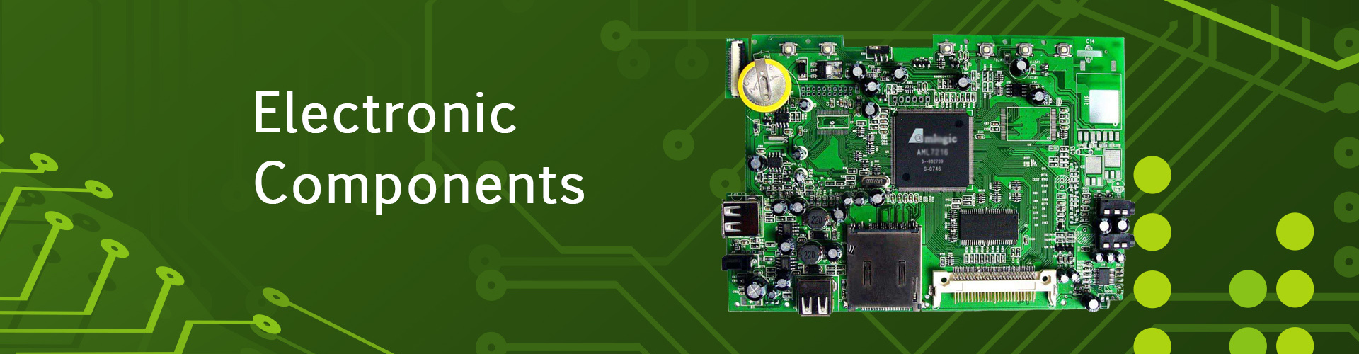


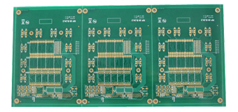
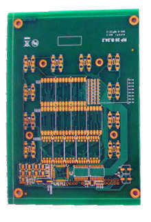
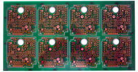
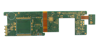
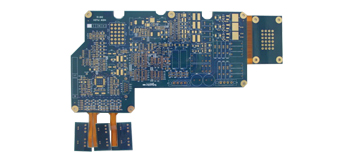
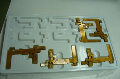
Bare PCB/FPC
Layer count |
1 ~ 64layers |
|
|
Laminates type |
FR-4(High Tg, Halogen Free, High Frequency) FR-5, CEM-3, PTFE, BT, Getek, Aluminium base,Copper base,KB, Nanya, Shengyi, ITEQ, ILM, Isola, Nelco, Rogers, Arlon |
||
Board thickness |
6-240mil |
||
Max Base copper weight |
210um (6oz) for inner layer 210um (6oz) for outer layer |
||
Min mechanical drill size |
0.2mm (0.008") |
||
Aspect ratio |
12 : 1 |
||
Max panel size |
Sigle side or double sides:500mm*1200mm, Multilayer layers:508mm X 610mm (20" X 24") |
||
Min line width/space |
0.076mm / 0.0.076mm (0.003" / 0.003") |
||
Via hole type |
Blind / Burried / Plugged(VOP,VIP…) |
||
HDI / Microvia |
YES |
||
Surface finish |
HASL Lead Free HASL Immersion Gold (ENIG), Immersion Tin, Immersion Silver Organic Solderability Preservative (OSP) / ENTEK Flash Gold(Hard Gold plating) ENEPIG Selective Gold Plating, Gold thickness up to 3um(120u") Gold Finger, Carbon Print, Peelable S/M |
||
Solder mask color |
Green, Blue, White, Black, Clear, etc. |
||
Impedance |
Single trace,differential , coplanar impedance controlled ±10% |
||
Outline finish type |
CNC Routing; V-Scoring / Cut; Punch |
||
Tolerances |
Min Hole tolerance (NPTH) Min Hole tolerance (PTH) Min Pattern tolerance |
±0.05mm ±0.075mm ±0.05mm |
|
Sort |
Item |
Normal capability |
Specific capability |
|
Layer count |
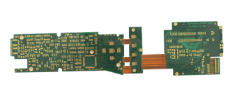
Rigid-flex PCB |
2 ~14 |
2 ~24 |
|
Flex PCB |
1 ~10 |
1 ~12 |
||
Board |
Min. Thickness |
0.08 +/- 0.03mm |
0.05 +/- 0.03mm |
|
Max. Thickness |
6mm |
8mm |
||
Max. Size |
485mm * 1000mm |
485mm * 1500mm |
||
Hole & Slot |
Min.Hole |
0.15mm |
0.05mm |
|
Min.Slot Hole |
0.6mm |
0.5mm |
||
Aspect Ratio |
10 : 1 |
12 : 1 |
||
Trace |
Min.Width / Space |
0.05 / 0.05mm |
0.025 / 0.025mm |
|
Tolerance |
Trace W / S |
± 0.03mm |
± 0.02mm |
|
Hole to hole |
± 0.075mm |
± 0.05mm |
||
Hole Dimension |
± 0.075mm |
± 0.05mm |
||
Impedance |
0 ≤ Value ≤ 50Ω : ± 5Ω 50Ω ≤ Value : ± 10%Ω |
|||
Material |
Basefilm Specification |
PI : 3mil 2mil 1mil 0.8mil 0.5mil |
||
ED&RA Cu : 2OZ 1OZ 1 / 2OZ 1 / 3OZ 1 / 4OZ |
||||
Basefilm Main supplier |
Shengyi / Taiflex / Dupont / Doosan / Thinflex |
|||
Coverlay Specification |
PI : 2mil 1mil 0.5mil |
|||
LPI Color |
Green / Yellow / White / Black / Blue / Red |
|||
PI Stiffener |
T : 25um ~250um |
|||
FR4 Stiffener |
T : 100um ~2000um |
|||
SUS Stiffener |
T : 100um ~400um |
|||
AL Stiffener |
T : 100um ~1600um |
|||
Tape |
3M / Tesa / Nitto |
|||
EMI shielding |
Silver film / Copper / Silver ink |
|||
Surface finish |
OSP |
0.1 - 0.3um |
||
HASL |
Sn : 5um - 40um |
|||
HASL(Leed free) |
Sn : 5um - 40um |
|||
ENEPIG |
Ni : 1.0 - 6.0um |
|||
Plating hard gold |
Ni : 1.0 - 6.0um |
|||
Flash gold |
Ni : 1.0 - 6.0um |
|||
ENIG |
Ni : 1.0 - 6.0um |
|||
Immesion silver |
Ag : 0.1 - 0.3um |
|||
Plating Tin |
Sn : 5um - 35um |
|||
SMT |
Type |
0.3mm pitch Connectors |
||
0.4mm pitch BGA / QFP / QFN |
||||
0201 Component |
||||
- LAMINATE SHEAR
- INNERLAYER IMAGE
- I/L ETCHING
- AOI INSPECTION
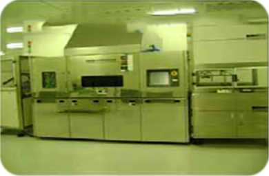
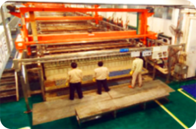
- LAMINATION
- DRILLING
- P.T.H.
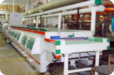
- PANEL PLATING
- OUTERLAYER IMAGE
- PATTERN PLATING
- O/L ETCHING
- INSPECTION
- LIQUID S/M
- SCREEN LEGEND
- Immersion gold
- FINAL SHAPING
- ELECTRICAL TEST
- VISUAL INSPECTION
- O.Q.C
- PACKING&SHIPPING
-
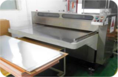
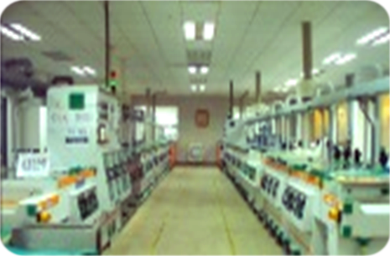
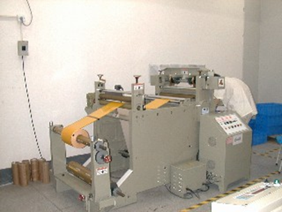
Auto material cutting machine, cut sheet size 37*49inch, 41*49inch, 43*49inch to working PNL size.
Check point:
1.Base Material Type
2.Dimension
3.No Dent、No Scratch
4.Quantity -
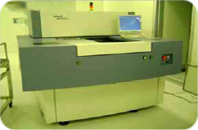
laser direct imaging
Check point:
1.Correct CAM data
Auto exposure machine
Check point:
1.Energy
2.Vacuity
3.Environment
Develop check point:
1.Temperature
2.Pressure
3.Concentration -
After development, the non-product copper is etched away.
Check point:
1.Temperature
2.Speed、Pressure
3.Concentration
4.Line width/space -
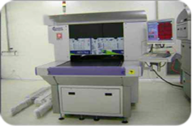
AOI(Automatic Optic Inspection)
Check point:
1.Open/short
2.Copper Residue -
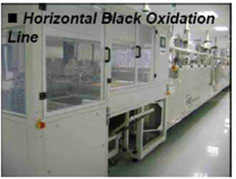
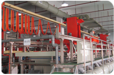
Horizontal black oxidation
Check point: 1.Concentration 2.Temperature 3.Coating ThinknessVertical black oxidation
Check point: 1.Concentration 2.Etching Rate 3.TemperatureVacuum high-presure laminated machine
Check point: 1.Temperature 2.Temp. increase Rate 3. Pressure
Quality check point: 1.Board Thinkness 2.Delamination 3.Appearance -
Mechanical drilling
Check point:
1.Hole Size
2.Hole Wall Roughness
3.Registration
4.The amount of holes
5.Appearance
Laser drilling, drill micro via holes
Check point:
1.Laser drill completely
2.Hole diameter寸
3.Hole shape -
Plasma desmer
Check point:
1.Plasma parameters
2.Mixed gas species
3.Power energy
4.Working pressure, processing time and gas flow rate
Plate through holes
Check point:
1.Temperature
2.Concentration
3.Plating Rate
4.Back Light Test -
Horizontal plating
Check point:
1.Temperature
2.Concentration
3.Current Density
Vertical plating
Check point:
1.Temperature
2.Concentration
3.Current Density -
laser direct imaging
Check point:
1.Correct CAM data
Auto exposure machine
Check point:
1.Energy
2.Vacuity
3.Environment -
Pattern plating
Check point:
1.Temperature
2.Concentration
3.Current Density
4.Check scratching the tin on the lines
Quality check point:
1.Hole Wall Thk.
2.Surface Copper Thk.
3.Apperance -
The non-product copper is etched away.
Check point:
1.Temperature
2.Speed
3.Pressure
3.Concentration
4.Line width/space -
AOI(Automatic Optic Inspection)
Check point:
1.Open/short
2.Copper Residue -
Spry coating line
Check point:
1.No Exposure copper
2.No Mask on Pad
3.No Scratch, Scum -
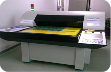
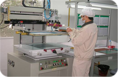
Auto-printing
Check point:
1.correct CAM data
2.Registration
3.Definition
4.No scratching -
Immersion Gold
Check point:
1.Temperature
2.Concentration
Quality check point:
1.Au / Ni thickness
2.Phosphorus percent
3.Apperance
Hot air leveling
Check point:
1.Angle of Air Knives
2.Solder Bath Temp.
3.Air Knives Temp.
Quality check point:
1.Sn/Pb Thinkness
2.Apperance -
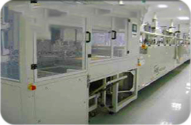
CNC routing for finish board size
Check point:
1.Dimension
2.No Powder Residue
3.No Scratch -
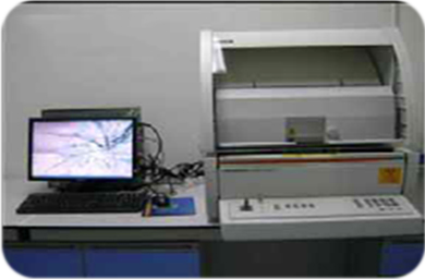
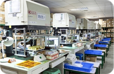
Flying probe tester
Check point:
1.Open
2.Short
3.Circumferential Separation -

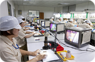
Fanal quality control, visual inspection
Check point:
1.Scratching
2.Crease 3.Oxidation
4.Solder deviation
5.Drill deviation
6.Conductor nick
7.Copper residue and so on -
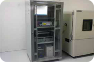
SIR Oven
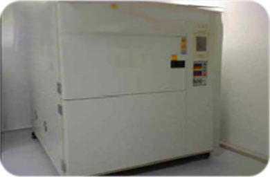
Surface insulation resistance testingThermal cycling chamber
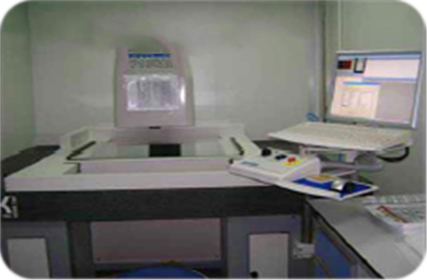
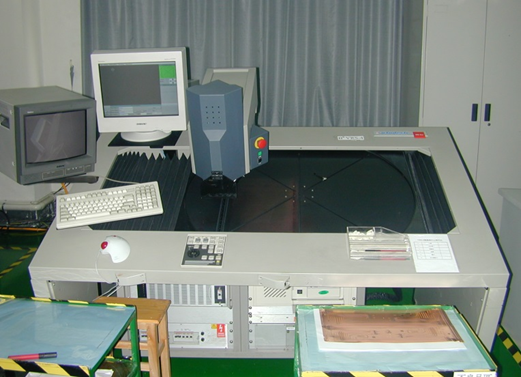
Thermal cycling testing3D Dimension
X-ray measuring instrument Measuing gold thickness, nickel thickenss, solder thickness and so on
- Cutting
- D/F Lamination & Exposure
- D.E.S.
- AOI
- CVL Lamination
- Black / brown oxygen
- Lay up
- Laminating
- NC Drilling
- Plasma
- P.T.H
- D/F Lamination & Exposure
- D.E.S.
- LPI
- Surface finish
- Silksreen
- E.T
- Assembling
- Punching/Routing
- FQC
- Packing
-
Cutting:
Coil material cutting piece material
Check Ponit:
Dimension/Thickness -
D/F Lamination & Exposure:
Graphic transfer
Check Ponit:
Film transmittance/expansion/contraction/appearance and revision -
D.E.S:
Graphic transfer
Check Ponit:
Trace width/Trace space/open/short -
AOI:
Automated Optical Inspection
Check Ponit:
Open/Short -

Coverlay:
Paste insulation protective film
Check Ponit:
Missing opening/Offset/Excessive glue/CL On pad/Dust/Copper Exposed -
Black/brown oxygen:
To increases the joint force between each layer for mulitlayer -
Lay up:
Stack up each layer for multilayer
Check Ponit:
Offset/Foreign matter -

Lamination:
By high temperature and high pressure makes each layer get together
Check Ponit:
Thickness/Delamination/Layers of board -
NC Drilling:
Drill hole for basefilm/stiffener/coverlay
Check Ponit:
Hole diameter/degree of deviation/quanity of holes -
Plasma:
Desmear process -
PTH:
Ensure the conduction of each layer
Check Ponit:
Copper thickness and back light -
D/F Lamination & Exposure
:Graphic transfer
Check Ponit:
Film transmittance/expansion/contraction/appearance and revision -
D.E.S:
Graphic transfer
Check Ponit:
Trace width/Trace space/open/short -
LPI:
Print solder resist ink
Check Ponit:
SM on pad/Missing SM/SM off normal/Dust/No developing cleanness -
Surface finish:
Plating metal protective film on pads,it's protect pads,and convenient in SMT
Check Ponit:
Exposured copper/Gold thickness -
Silksreen:
Print Comp Symbols and logos on board
Check Ponit:
Legend on pad/Legend obscure -
ET:
Ensure electrical function, avoid open/short circuit
Check Ponit:
Open/Short -

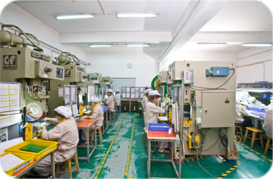
Assembing:
Paste Stiffener(PI/FR4/AL/SUS) and tape
Check Ponit:
Offset/Excessive glue/Dust -
Punching/Routing:
Cutting the profile of board
Check Ponit:
Dimension -
FQC:
Final Quality Control For Product
Check Ponit:
Appearance inspection -
Packing:
Protection products, to avoid damage in transit